Our research
The STEM group at the Laboratoire de Physique des Solides explores nano to atomic scale physics with ultra-high energy resolution electron spectroscopy
Our equipment
We are equiped with state of the art. We are equiped with state of the art electron spectro microscopes fitted with various home-made cutting edge developments permitting original EELS, cathodoluminescence, PINEM or 4D microscopy modes.
Our networks
We are part of several french and european networks and projects.
Latest news and research highlights
-
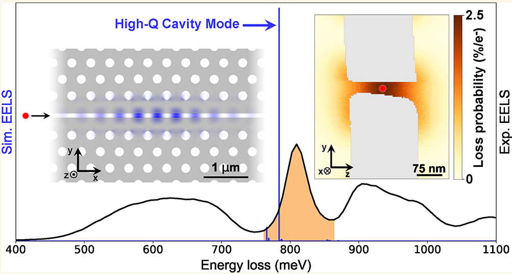
High-Efficiency Coupling of Free Electrons to Sub‐λ cube Modal Volume, High‐Q Photonic Cavities
We report on the design, realization, and experimental investigation by spatially resolved monochro- mated electron energy loss spectroscopy (EELS) of high- quality-factor cavities with modal volumes smaller than λ3, with …
-
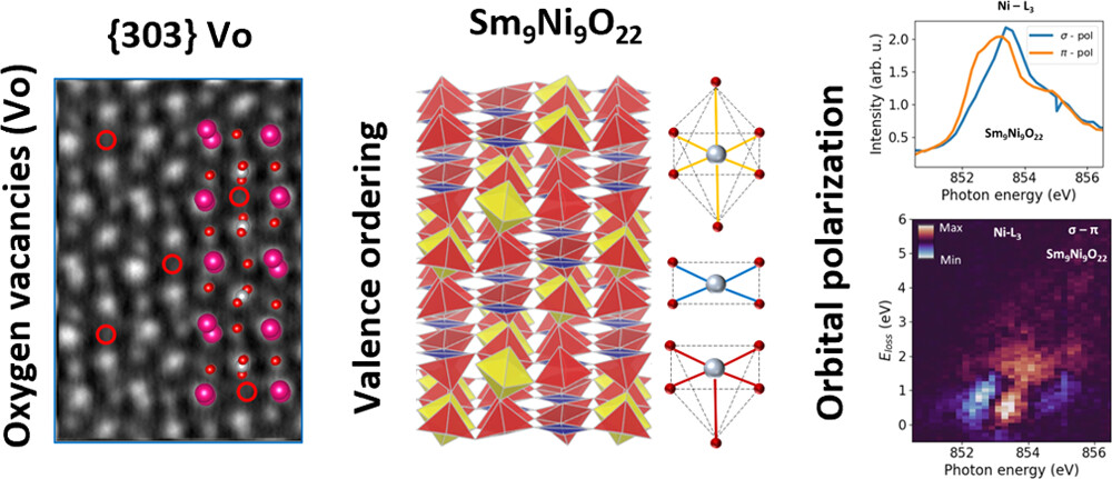
Valence-Ordered Thin-Film Nickelate with Tri-component Nickel Coordination Prepared by Topochemical Reduction
In a groundbreaking study, researchers have synthesized Sm9Ni9O22 using the metal-hydride-based “topochemical reduction” process. This compound exhibits ordered nickel valences associated with tri-component coordination configurations, resulting in a unique crystal …
-
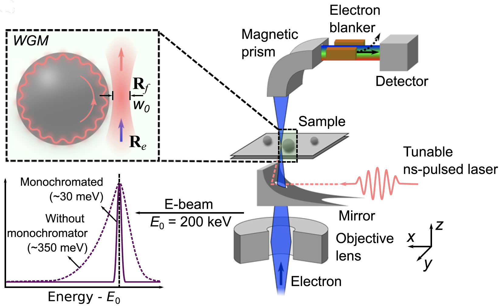
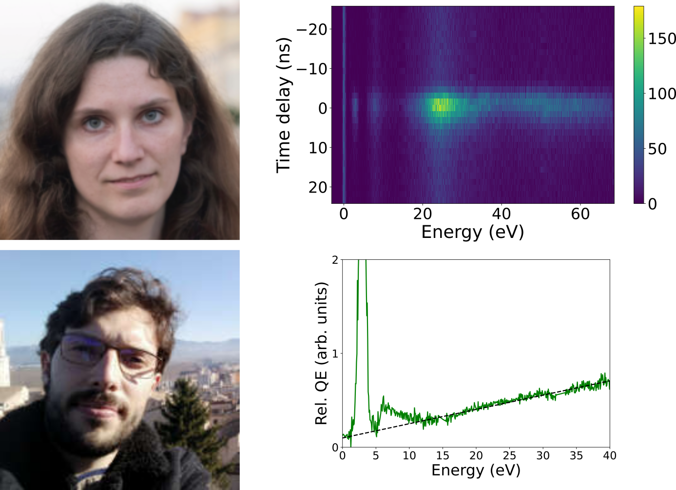
μeV electron spectromicroscopy using free-space light
The synergy between free electrons and light has recently been leveraged to reach an impressive degree of simultaneous spatial and spectral resolution, enabling applications in microscopy and quantum optics. However, …
-
We are in Linkedin
Stay in the loop with all the latest happenings of our group! Follow our LinkedIn page to stay up-to-date with the most recent updates and news. Join us on this …
-
EMS OPA 2022 Instrumentation and Technique Development prize for Cathodoluminescence Excitation Spectroscopy (CLE)
Congratulations to Nadezda Varkentina, Yves Auad and co-authors who have received the EMS OPA 2022 Instrumentation and Technique Development prize for their work entitled “Cathodoluminescence excitation spectroscopy: Nanoscale imaging of …
-
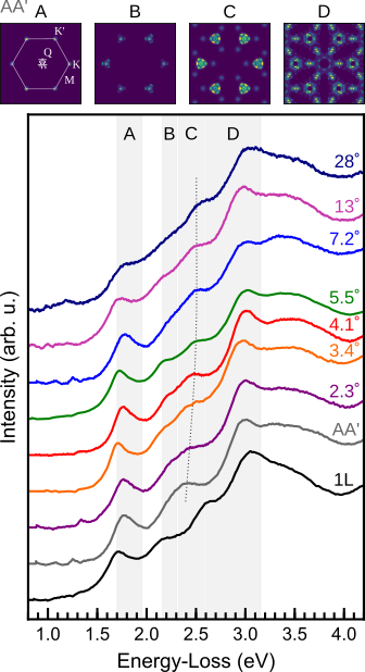
Excitonic absorption signatures of twisted bilayer WSe2 by electron energy-loss spectroscopy
Moiré twist angle underpins the interlayer interaction of excitons in twisted van der Waals hetero- and homostructures. The influence of twist angle on the excitonic absorption of twisted bilayer tungsten …
Open positions
-
Master internship: Investigation of biomineral formation by analytical microscopy at high spectral resolution.
-
Master 2 internship: STEM-EELS and 4D-STEM Characterization of Quantum Materials and Interfaces
-
Post-doc position : Electric-field-activated metal/insulator transitions in Cr-V2O3 investigated by in situ electron spectromicroscopy techniques
-
Ph D and post-doc positions: Exploring the physics of 2D materials excitations using relativistic electrons
Latest publications
PRB Editors’ Suggestion: #Excitonic #absorption signatures of twisted bilayer
#WSe2 by #ElectronEnergyLossSpectroscopy
S. Y. Woo, A. Zobelli, R. Schneider, A. Arora, J. A. Preuß et al.,
Phys. Rev. B 107, 155429
➡️ https://go.aps.org/41RW5cf
#EdSugg #condmat @APSPhysics @STEM_LPS
Folds and wrinkles in boron nitride (BN) sheets can locally reduce the band gap and may trap charge carriers, find researchers from @STEM_LPS and @chrisewels group
Interested in working on the best monochromated #ElectronMicroscopy and challenging it with #Synchrotron based spectroscopy? Check out our #PhD scholarship where such outstanding tools will be combined to investigate 2D electron gases at oxide interfaces! https://www.stem.lps.u-psud.fr/2d-gases-oxide-nanostructures-revealed-high-space-energy-and-momentum-resolved-spectroscopy